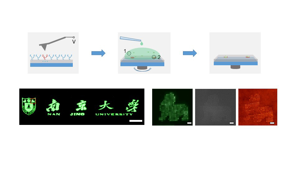

Scientists and engineers have dreamed for decades of fast, low-cost, reliable, and multi-component nanopatterning techniques for printing functional colloidal nanoparticles. Although countless efforts have been devoted, it is still a daunting challenge to organize different nanocomponents into a predefined structure with nanometer precision over millimeter scale without forming defects. We have developed a nanoprinting technique, which utilizes a tip-based high-voltage writing process to generate nanoscale charged patterns on the substrates (Fig. 1a). This process not only enables electrostatic trapping but also creates a high local surface potential in contrast to the uncharged area, both favoring highly efficient site-specific NP assembly (Fig. 1b).

Fig. 1| a, Schematic illustration of the nanoparticle printing process which involves high-voltage electrostatic nanopattern generation, surface modification, and site-specific NP assembly by electrical trapping. b, Electrical trapping potential in a nonpolar solvent as a function of the distance from the center of the written charge. The electric fields can extend for hundreds of nanometers, leading to the high efficiency of NP collection. c, Surface potential modulation along the nanopattern surface. De-fluorination through high voltage induces significant surface energy modulation, providing strong short-range interactions to fix the NPs.
Print nanoparticles into defined patterns with a 200 nm pitch (~125,000 DPI), 30 nm (or larger) pixel size, 10 nm position accuracy in millimeter scale, with minimum error (error ratio < 2×10⁻⁶)
With our developed method, we can accurately assemble perovskite quantum dots (QDs) in an area of 100×800 μm2, as shown in the photoluminescence (PL) image of “Nanjing University” Logo, composed of 9481 pixels, approximately 4.7×10⁵ 10-nm CsPbBr3 NPs (Fig. 2a,b). No nonspecific adsorption was found in the uncharged area. In other words, the error ratio (i.e., the ratio of the number between nonspecific adsorbed and correctly printed NPs) is lower than 2×10⁻⁶. Moreover, the printing technique enjoys a very high resolution and accuracy. The pitch size can reach 200 nm (125, 000 DPI), or even a smaller value, as supported by the Kelvin probe force microscope (KPFM) potential maps and the corresponding AFM height maps of the printed structure (Fig. 2c). This has exceeded the diffraction limit of light and can potentially allow direct printing of metasurface-like structures in the optical regime.

Fig. 2| a, A large-scale photoluminescence (PL) image obtained by printing CsPbBr3 NPs, with a total area of 100 × 800 μm2. Scale bar, 50μm. b, High-magnification PL, SEM, and AFM height images of the marked area in Fig. a. Scale bar, 2 μm. c, High-magnification KPFM potential map and corresponding AFM height map after NP assembly with a pitch of 200 nm. Scale bar: 500 nm.
Print multiple functional nanoparticles
The combinational patterning of different nanoparticles can be achieved by repeating the writing/deposition cycles. We printed a pseudo-color image with four different NPs, with 15-nm Fe2O3 NPs being used for creating the white color, and NaYF4:Yb,Er, CsPbBr3, and CdSe@ZnS NPs for magenta, green and red colors in the image captured by the dark-field microscopy (Fig. 3). No cross-contamination is observed in each pixel, further confirming the robustness of the method for printing multiple functional NPs. To the best of our knowledge, this is the first time that true color nanoprinting is achieved.

Fig. 3| a, Darkfield images of each step in the four-cycle overlay procedures. The KPFM potential images in the insets show the surface potentials at the corresponding cycles. b, Pseudo-color image captured by dark-field microscopy of a color pattern, white color is created by 15-nm γ-Fe2O3 NPs, while magenta, green and red colors are produced by NaYF4:Yb,Er, CsPbBr3 and CdSe@ZnS NPs. Scale bar, 10 μm.
We believe this technique provides a powerful yet straightforward construction tool for large-scale positioning and integration of multiple functional nanoparticles toward next-generation photonics, optoelectronic, and biomedical devices.


Please sign in or register for FREE
If you are a registered user on Research Communities by Springer Nature, please sign in