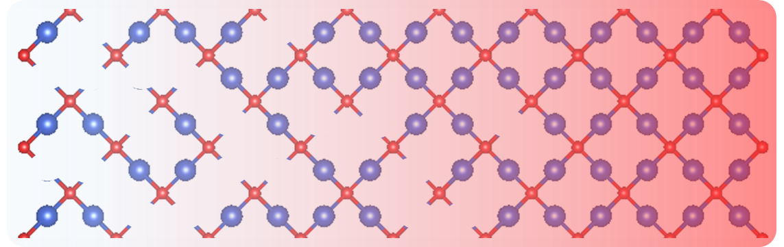
My relationship with Spatial Atomic Layer Deposition (SALD), and with ALD in fact, dates back to early 2009, when I was a postdoc working with Prof. Judith MacManus-Driscoll at the Device Materials Group in the Materials and Metallurgy Department of the University of Cambridge. After receiving a couple of close-proximity SALD systems from Kodak, my objective was to further develop and optimize them to deposit oxide thin films as components for new generation solar cells, given SALD is a low-cost, non-vacuum, high-throughput scalable technique. This is so thanks to the continuous injection of precursors, which are separated in space (i.e. in different locations of the reactor), as opposed to the sequential injection of conventional ALD.1 SALD had just been brought back to life by Kodak and TNO, despite the early ALD patents by T. Suntola in 1977 (where he described the spatial ALD concept) and 1983 (where he showed that the spatial concept could be applied at atmospheric pressure using metalorganic precursors).2
At the time, three Ph.D. students in the group (Kevin Musselman, now a professor at the University of Waterloo, Canada, with whom I continue collaborating in the development of the SALD technique, Talia Gershon and Andrew Marin) were performing exciting work on ultra-low cost all-oxide solar cells based on ZnO and Cu2O. The deposition of Cu2O by SALD not being reported, it was thus an obvious challenge to take on to contribute to the research efforts of my fellow PhDs in the team. Surprisingly, and given how much Cu2O has been studied, there were indeed very few papers dealing with the deposition of Cu2O by conventional ALD from which we could get a starting point. With the help of Luke Dunlop (another bright Ph.D. student in the group), we narrowed down the choice of precursor to Cu(hfac)(tmvs) (copper hexafluoroacetylacetonate trimethylvinylsilane, also commercialized as Cupraselect). This precursor contains Cu in the +1 oxidation state and, although it had been mainly used to deposit metallic copper, previous studies showed that it could be hydrolyzed by water to yield Cu2O. As it turned out (and with the help of undergrad students Catriona Yeih and Matthew Jordan), we manage to deposit Cu2O thin films at low temperatures (below 225 °C) that had surprisingly outstanding transport properties. For example, mobility values of ~6 cm²/Vs were obtained at 225 °C, comparable to the values obtained by thermal oxidation at 400 °C, with two orders of magnitude faster deposition rate as compared with ALD. The results were published,3 and the films were used to improve the performance and get insight on the device physics of electrodeposited ZnO/Cu2O solar cells.4 But the reason why SALD Cu2O thin films were so good was still to be worked out.
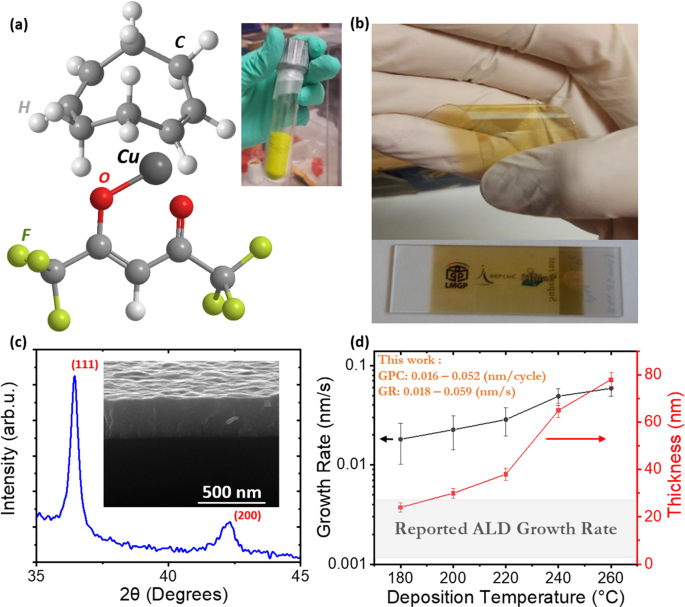
Then in 2013, I got a permanent position at the LMGP (Laboratoire des Matériaux et du Génie Physique, a joint unit between Grenoble INP, within the University of Grenoble Alpes, and the CNRS) in Grenoble, France. One axis of my research focused (still does) on the development of the SALD technique in the lab. I thus set about designing and building a new close-proximity reactor based on the approach by Kodak, and one of my main objectives was to continue working with copper-based materials and try to understand the good transport properties we had obtained for Cu2O in Cambridge. Although Cupraselect had proven to be a good choice, the fact that it is not a very stable precursor prompted me to look for an alternative, more stable one. During one of the different occasions I had to exchange with Simon Rushworth, an expert in ALD/CVD precursors and their chemistry, he suggested using a similar precursor, Cu(hfac)(cod) (cod: cyclooctadiene). Although effectively more stable, this precursor is solid and has a low vapour pressure, which is a serious drawback when working with a SALD system operating in the open air, such as ours. In addition, it had never been used to deposit Cu2O by CVD or ALD. We nevertheless gave it a try and managed to deposit some Cu2O thin films (as part of the work of Ph.D. students Cesar Masse de la Huerta and Viet Huong Nguyen, who is now a permanent researcher in Vietnam where he continues working in SALD).
This initial work was taken over by Ph.D. student Abderrahime Sekkat (in front or our home-made SALD system in the image in Figure 1), whose thesis focuses on Cu2O based energy devices. To our surprise, the Cu2O thin films deposited with the new solid precursor showed even better transport properties. As detailed in our Nature Materials Communications paper, mobility values above 90 cm2/Vs (i.e similar to those obtained in Cu2O single crystals) have been obtained for films deposited at 260 °C (mobility values obtained at 180 °C being around 30 cm2/Vs).5 This was again an excellent result but, still, we had no clue why SALD Cu2O films were so good. This is where Raman spectroscopy came to the rescue. Although Raman Spectroscopy is commonly used to probe the crystalline phase of oxides, in the case of Cu2O, it provides a key insight into the defects present in the material. This had been recently demonstrated in an insightful work by T. Sander,6 who showed that the Raman spectrum of Cu2O should contain very few peaks. The extra peaks observed are indeed caused by a perturbation of the symmetry as a result of the presence of defects. We could see that as the deposition temperature increased, the peaks associated with defects (in particular Cu vacancies, see the paper for details) decreased, which results in enhanced mobility. Raman data thus allowed us to understand why films made from both precursors at the same temperature showed such different transport properties (orders of magnitude difference in mobility), just by taking a look at the intensity of the peaks related to defects in the Raman spectra (see Figure 1).
(cod) and Cu(hfac)(tmvs). A clear difference of intensity of the peaks related to defects can be observed")
Thanks to the excellent and hard work Abdou is carrying out during his PhD thesis, we have been able to show how our Cu2O films can be used in Silicon solar cells, obtaining record efficiencies in large-area devices.7 We are also now able to easily tune the carrier concentration/mobility of the films, and to deposit CuO and Cu thin films with our system at low temperatures. These results are to be published soon, so stay tuned!
References
(1) Muñoz-Rojas, D.; Macmanus-Driscoll, J. Spatial Atmospheric Atomic Layer Deposition: A New Laboratory and Industrial Tool for Low-Cost Photovoltaics. Mater. Horizons 2014, 1 (3), 314–320. https://doi.org/10.1039/c3mh00136a.
(2) George, S. M. Atomic Layer Deposition: An Overview. Chem. Rev. 2010, 110 (1), 111–131. https://doi.org/10.1021/cr900056b.
(3) Muñoz-Rojas, D.; Jordan, M.; Yeoh, C.; Marin, A. T.; Kursumovic, A.; Dunlop, L. A.; Iza, D. C.; Chen, A.; Wang, H.; MacManus Driscoll, J. L. Growth of ∼5 Cm2V-1s-1 Mobility, p-Type Copper(I) Oxide (Cu2O) Films by Fast Atmospheric Atomic Layer Deposition (AALD) at 225°C and Below. AIP Adv. 2012, 2 (4). https://doi.org/10.1063/1.4771681.
(4) Marin, A. T.; Muñoz-Rojas, D.; Iza, D. C.; Gershon, T.; Musselman, K. P.; MacManus-Driscoll, J. L. Novel Atmospheric Growth Technique to Improve Both Light Absorption and Charge Collection in ZnO/Cu2O Thin Film Solar Cells. Adv. Funct. Mater. 2013, 23 (27), 3413–3419. https://doi.org/10.1002/adfm.201203243.
(5) Sekkat, A.; Nguyen, V. H.; Arturo, C.; La, M. De; Rapenne, L.; Bellet, D.; Kaminski-cachopo, A.; Chichignoud, G.; Muñoz-rojas, D. Open-Air Printing of Cu2O Thin Films with High Hole Mobility for Semitransparent Solar Harvesters. Commun. Mater. 2021, 2 (10.1038/s43246-021-00181–8). https://doi.org/10.1038/s43246-021-00181-8.
(6) Sander, T.; Reindl, C. T.; Giar, M.; Eifert, B.; Heinemann, M.; Heiliger, C.; Klar, P. J. Correlation of Intrinsic Point Defects and the Raman Modes of Cuprous Oxide. Phys. Rev. B - Condens. Matter Mater. Phys. 2014, 90 (4), 1–8. https://doi.org/10.1103/PhysRevB.90.045203.
(7) Nguyen, V. S.; Sekkat, A.; Bellet, D.; Chichignoud, G.; Kaminski-cachopo, A.; Muñoz-Rojas, and D.; Favre, W. Open-Air, Low-Temperature Deposition of Phase Pure Cu2O Thin Films as Efficient Hole-Transporting Layers for Silicon Heterojunction Solar Cells. J. Mater. Chem. A 2021, No. 10.1039/d1ta02931b. https://doi.org/10.1039/d1ta02931b.


Please sign in or register for FREE
If you are a registered user on Research Communities by Springer Nature, please sign in