The next generation wireless communication technology calls for integrated radiofrequency devices capable of operating at frequencies beyond 90 GHz. Currently, the two semiconductor technologies most used for RF devices are silicon complementary metal-oxide-semiconductor (CMOS) field-effect transistors (FETs) and transistors based on III-V compound semiconductors (primarily GaAs). Unfortunately, both semiconductor RF technologies can not provide satisfied high operating frequency and high integration level simultaneously.
Owing to high carrier mobility and saturation velocity, ultra-small intrinsic capacitance, excellent stability and thermal conductivity, semiconducting single-wall carbon nanotubes (CNTs) are considered as a promising candidate in high-speed FETs up to terahertz (THz) frequencies. Originating from the unique transport properties and density of states, CNTs are predicted to result in high inherent linearity in transistors. Additionally, the materials requirements of CNTs for RF/analog and digital devices are basically the same. Therefore, CNT FETs could make a better platform for SoC applications than silicon and III-V compound semiconductors based technologies.

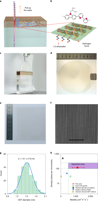
Fig. 1| Preparation of aligned semiconducting CNT arrays. a,b, Schematic diagrams illustrating a binary liquid interface-confined self-assembly (BLIS) procedure. c,d, Optical images showing an as-deposited 4-inch quartz wafer (c) and square glass substrate (d). e, SEM image showing an as-deposited CNT arrays on a silicon substrate. f, Benchmarking density and carrier mobility of CNT arrays from this work and other reported CNT arrays.
However, both speed and gain of CNT FETs still lag behind theoretical predictions. Speed improvement is principally hindered by the lack of well-aligned semiconducting CNT arrays with suitable density, high uniformity, high semiconducting purity and high carrier mobility. In our recent work in Nature electronics, we report a new method based on double-dispersion and binary liquid interface-confined self-assembly (BLIS) procedure, adapted from an existing DLSA method, which allows for assembly of aligned arrays on both insulating or semiconducting substrates, such as silicon, glass and quartz. After the thorough characterization, we find that our CNT arrays surpass all other reported CNT arrays in terms of more suitable density and higher carrier mobility, and thus are the most promising CNT material system to date for constructing high-speed RF transistors.
First, we fabricate the RF FETs on the quartz substrate due to its ultralow high-frequency loss. These transistors show the expected excellent extrinsic (as-measured) frequency performance. Although insulating substrate helps to reduce parasitics of FETs, the frequency performance of CNT FETs is dragged down due to the lower achievable CNT density on quartz (70 CNTs/μm) than on silicon substrate (120 CNTs/μm). To explore the speed potential of CNT arrays-based FETs, we fabricated FETs on high-resistivity Si substrates with well-designed structures through an optimized fabrication process. The 50 nm-Lg transistors exhibit the record frequency performance. Extending the fitted linear fT,INT - Lg-1 line to shorter channel length, the intrinsic cut-off frequency of CNT arrays-based FETs is expected to reach 1 THz at Lg = 28 nm, demonstrating the great potential of CNT arrays-based high-speed electronics for THz applications. While it was long predicted theoretically that CNT FETs have THz potential, this is the closest experiment demonstration.

Fig. 2| RF transistors and amplifiers based on aligned semiconducting CNT arrays. a, Benchmarking of intrinsic fT versus Lg between our CNT FETs and those of other CNT and graphene transistors. The extrapolating dash line suggests that intrinsic fT = 1 THz should be achieved with our FETs as Lg is scaled down to 28 nm. b, Comparison of intrinsic fT versus fMAX between this work and those reported for CNT and graphene transistors. c, Output power versus input power curves for a single-tone test. d, Output power versus input power curves for the linearity test.
Finally, we demonstrate the well-designed multi-finger CNT arrays-based FETs to increase total output power. Benefiting from the low output d.c. resistance of our FET, the maximum power gain reaches 11.70 dB even under the standard 50 Ω impedance matching condition. We also demonstrate RF amplifiers with a power gain of 23.2 dB and high inherent linearity (IIP3 and OIP3 of 20.6 dBm and 31.2 dBm, respectively) up to 18 GHz.
By integrating with high-performance digital CNT-based CMOS ICs, CNT arrays-based high-speed electronics could become competitive with conventional semiconductor technology for SoC applications operating in millimetre wave and even THz frequencies.
If you are interested in more details of our work, please refer to the paper published in Nature Electronics: “ Radiofrequency transistors based on aligned carbon nanotube arrays ” following the link: https://www.nature.com/articles/s41928-021-00594-w


Please sign in or register for FREE
If you are a registered user on Research Communities by Springer Nature, please sign in