
Two-dimensional (2D) materials are not fresh news anymore. Yet the flat world is far from being fully explored and will continue delivering further discoveries and surprises. Not only there is a large selection of individual 2D materials (which is also constantly growing in number), but the amount of different combinations of them is overwhelming. Van der Waals (vdW) heterostructures with their endless variations can effortlessly provide enough physics phenomena to study for a lifetime of an army of eager researchers.
A great deal of the involved physics in these vdW hybrids brings up new ideas for various spintronic applications. Spintronics or spin transport electronics is a field of research that has revolutionized the computer industry and memory technology, giving rise to the emergence of hard disc drives and magnetoresistive random-access memories (MRAM). Spintronic devices are built with the purpose of transferring information with the spin of electrons which are supposed to operate faster and with less energy dissipation.
The idea behind MRAMs is based on the giant magneto-resistance effect (GMR), the discovery of which was awarded a Nobel prize in 1980 [1, 2]. According to the GMR effect, if you make a heterostructure of two ferromagnetic materials, separated by a non-magnetic layer and apply a charge current through it, the vertical charge transport is going to experience two different resistance levels, depending on whether the magnetization directions of the ferromagnetic layers are parallel or anti-parallel. These low and high resistance levels in the parallel and anti-parallel states define the spin-logic action and can be interpreted by computers as bits 0 and 1. Inspired by that, we thought about the possibility of mimicking this behavior in the 2D limit of our graphene-based heterostructures.

By the ongoing miniaturization process of making ever smaller and yet faster devices, nowadays spintronic circuitries are leaning towards employing atomically thin materials. An appropriate material should not only be a good electron conductor and have high spin-polarization of charge current (like a metallic ferromagnet), but should also preserve spin information over long enough distances. For the latter, graphene is an excellent choice showing exceptionally long-distance spin transport (tens of micrometers). However, it intrinsically has zero spin-polarization of charge current. Thus, in the original samples made by our group, the spins were injected into graphene by bulk ferromagnetic electrodes and graphene was merely playing the role of a spin transporter.
Over time with the progress in the field, we added more and more 2D ingredients into our dish. It turned out that by bringing other 2D materials in the close neighborhood of graphene, we are practically able to design a new material with the combined properties of each individual layer in the stack. Therefore, our main goal was to design a dream-like 2D heterostructure where the spins can be efficiently maintained and manipulated for the purpose of spin-logic functionality.
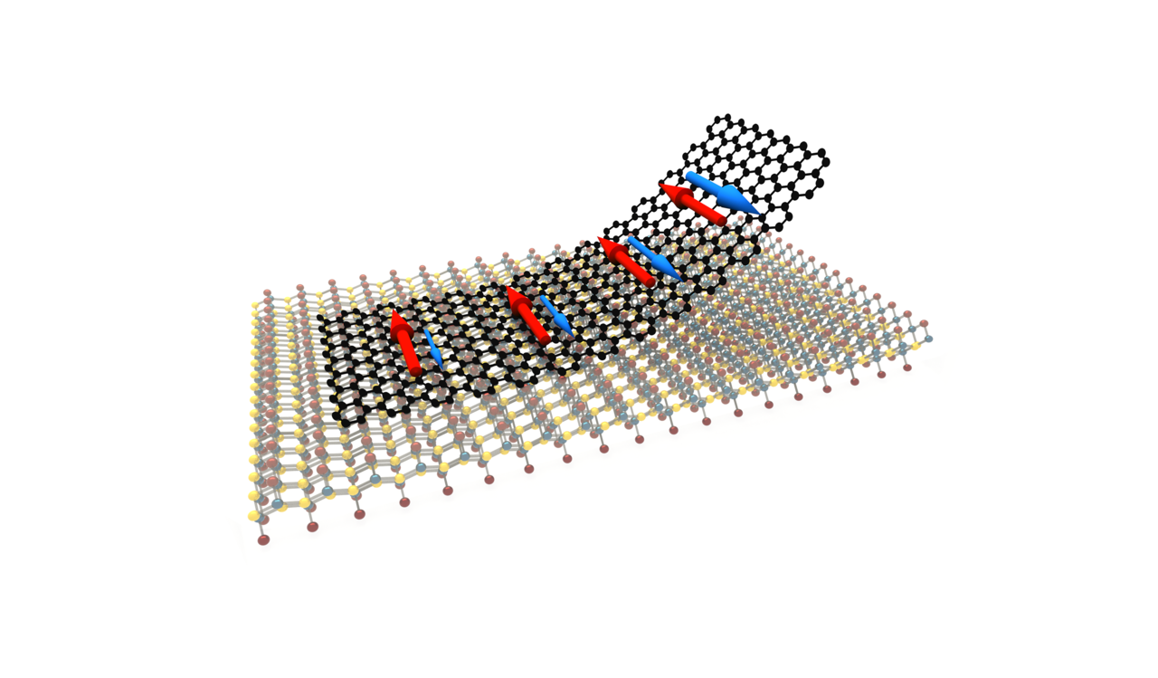
A layered antiferromagnetic material, such as CrSBr, is a very practical choice as a substrate for graphene particularly in the view of spin transport phenomena. Graphene on a CrSBr substrate becomes magnetic since it gains a considerable imbalance (as we found later ≈14%) in the number of spin-up and down electrons, while keeping its excellent transport properties intact. And this is all we wanted: high spin-polarization of charge current together with long-distance spin transport. The magnetic graphene can generate spin current, no matter if we apply a pure charge current to it or if we heat it up locally. This means that the magnetic graphene by itself can inject, transport, and detect the spin signal, opening the path for all-graphene spintronic circuitries. This sounds like we are getting closer to the ideal choice of material for the ultra-compact 2D spin-logic circuitry and magnetic memory/sensory devices.

Simplified schematic picture of the studied device, showing electrical and thermal generation of spin currents in a bilayer graphene/CrSBr van der Waals heterostructure. The magnetic Co electrodes are used to determine the degree of proximity induced spin polarization in the graphene, where the magnetization of the outer-most layer of CrSBr (MCSB) allows for higher conductivity of the spin-up electrons (red arrows).
We got to know about CrSBr in a GRC conference in July 2019 that initiated our collaboration with Columbia University, where the crystals were synthesized. Working with the air-stable CrSBr was quite easy, in contrast to many of the currently used magnetically ordered layered materials that are extremely sensitive to oxygen and humidity which immediately complicates all fabrication procedures. At the point when we started our research on CrSBr-based heterostructures, there was no report on spin transport in graphene in the proximity to it whereas the advantages of such a combination were clear.
When we measured a rather strange spin signal on the sample we were surprised by the strength of the proximity effect. The efficiency of the spin current generation was as large as that of conventionally used ferromagnetic electrodes! That was the beginning of endless days and nights of measurements of about 250 sweeps of all kinds of parameters (gate voltage, magnetic field, bias) all at different temperatures and orientation of the field that were supposed to be finalized in the course of 10 days. It was quite challenging but we were observing intriguing results and were scooping extra power from our fascination by the physics that we were lucky to behold. It was extremely fortunate that we finished our measurements just a couple of weeks before the full lockdown of the university in March 2020, when the whole world froze in a reaction to the pandemic. We brought the data analysis, analytical modeling and simulations home with us and started with drafting the manuscript. After a few months when the labs got reopened, more samples were measured with a lot of editing work to shape the final version of this publication. Now it is the moment for us to take one step further and design the spin-logic devices that are fabricated only from the layered materials, where the magnetic graphene by itself is performing the spin injection, transport, and detection! Realizing that we are very close to this achievement does not let us rest and gives endless motivation to deal with all the difficulties of the life of experimental physicists.
To read more about our work, please refer to the article published in Nature Nanotechnology; https://www.nature.com/articles/s41565-021-00887-3.
[1] Fert, Albert. "Nobel Lecture: Origin, development, and future of spintronics." Reviews of modern physics 80.4 (2008): 1517.
[2] Grünberg, Peter A. "Nobel Lecture: From spin waves to giant magnetoresistance and beyond." Reviews of Modern Physics 80.4 (2008): 1531.


Please sign in or register for FREE
If you are a registered user on Research Communities by Springer Nature, please sign in